“Semiconductor IP from Sofics enables higher IC performance, improves reliability and reduces design time and cost.”
Sofics specializes in creating Solutions for ICs at the forefront of semiconductor design and technology. We are committed to excellence in interfaces, PHYs, and I/Os, embodying our dedication to delivering uniquely valuable IP solutions.
We emphasize on the IC periphery, safeguarding and enhancing the core of your ICs with gold-standard solutions of unparalleled excellence. We elevate IC design by enhancing performance, ensuring superior reliability, and optimizing cost efficiency.
We are dedicated to innovation and committed to customer satisfaction. With Sofics IP you can break out of the boundaries of IC design and technology.
Sofics has three main product categories:
PhyStar: Robust circuit solutions
PhyStar® robust circuit and interface solutions, including custom digital I/O’s, circuits that handle transient disturbances (e.g. to provide antenna clipping or POR), as well as automotive standard PHYs (e.g. a full LIN PHY with integrated ESD, EOS and EMC robustness).
PowerQubic: On-chip ESD protection for high voltage and BCD processes
PowerQubic® on-chip ESD and EOS protection devices are suitable for high voltage CMOS/BCD, typically 0.35µm down to 55nm for voltage ranges from 5V to more than 50V; PowerQubic® IP is used in applications that need ESD clamps with a high holding voltage. Sofics designed on-chip ESD protection for several automotive, industrial applications where high robustness for a combination of harsh ESD, EOS, LU and EMI specs are part of the requirements.
TakeCharge: On-chip ESD protection for low voltage/advanced processes
TakeCharge® analog I/Os and on-chip ESD protection are available for low voltage CMOS from 0.25µm down to 2nm; These ESD protection solutions can be used for high-speed, low-leakage, low-capacitance, low-noise, RF, analog, over- and under voltage tolerance; often combined with beyond standard ESD robustness requirements.
“Interfaces and I/Os that safeguard and enhance the core of your ICs with gold-standard solutions”
Sofics Portfolio:

Our technology has been characterized on 11 foundries including advanced nodes at TSMC, UMC, GF, Samsung Foundry…
Our customers have integrated Sofics IP into thousands of IC designs across many different application verticals. Sofics IP is used in 40% of recent Bluetooth products, billions of smartphone imager chips, over a billion FPGA chips, most of the indoor positioning applications, in several car models and keys, optical communication modules for datacenters from multiple vendors and many other applications….
Engineering office
Sint-Godelievestraat 32, 9880 Aalter, Belgium
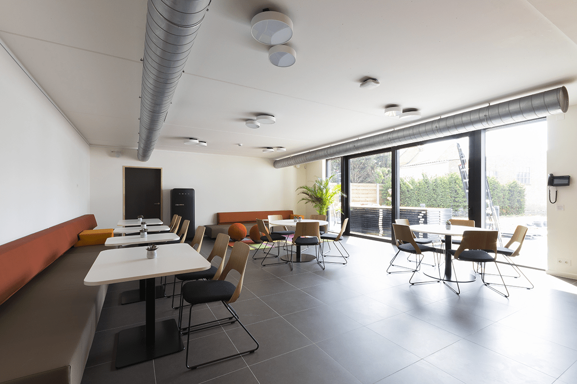
Our spacious, inspiring and energy-neutral office in Aalter is the ideal workplace for all kind of research and innovation.


