
Most foundries provide GPIO libraries free-of-charge that are perfect for the generic interfaces. Some applications however need specialty I/O circuits.
For 25+ years Sofics engineers have delivered unique ESD protection clamps to protect I/O circuits designed by the customer. More recently, Sofics has also designed functional I/O circuits, with ESD protection included.
ICs manufactured on advanced CMOS processes only support I/Os up to 1.8V. However, for communication with legacy chips higher voltages are required like 3.3V or even 5V.
Sometimes system makers demand high EOS and surge tolerance voltages, much beyond the foundry GPIO capabilities.
Contact us (info@sofics.com) to discuss your application.
We can provide the specialty I/O your chip needs.
Power-Performance-Area & Robustness (PPA & R)
Sofics GPIO circuits provide best PPA&R for each of the sub-blocks.
| GPIO-S | ESD | RX | TX | BIAS for multiple I/Os |
|---|---|---|---|---|
| Power | nW range | Below nW no leakage no static power | Physical limit in operation: CV²f. Below nW when not active (compared to uW for alternatives) | <uW – no static active currents |
| Performance | Sofics 25y track record Circuit and ESD co-design | Similar to regular GPIO limited delay (ns) despite OVT stack | Similar to regular GPIO limited delay (ns) despite OVT stack | Source & sink capable limited off-set error fit for OVT bias |
| Area | Sofics 25y track record Scales with ESD spec | DNW overhead according to design rule | Physical limit: CV²f Drive current (spec) n-stack: design rule | Decoupling cap spec: PDK specifies 20pF Sofics has a ~1pF option |
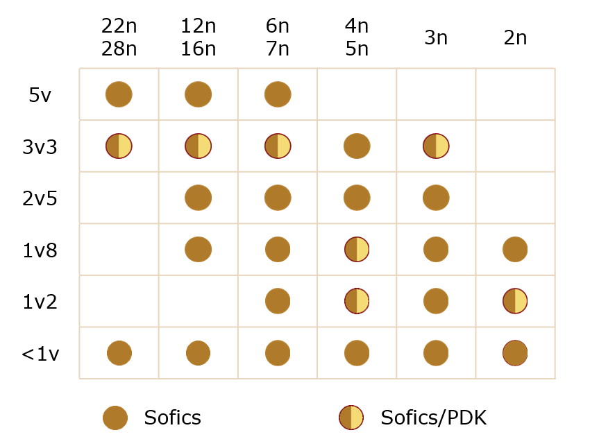
Examples in different processes
Examples on different process nodes are shown below. This is just a subset of cells proven on silicon and in mass production. Designs can be ported to other processes and adapted to your requirements.
As semiconductor technology scales down, the maximum tolerated voltage by the transistors is no longer sufficiently high to accommodate (older) I/O-standards. For instance, in 4nm FinFET technology, the maximum tolerated voltage during normal operation is limited to 1.2V, which does not support common bus standards like 1.8V. As depicted in the figure below, the advancements in the technology nodes, come with a decline in the maximum GPIO supply voltage, bringing in new design challenges.
Some examples from recent I/O projects
| I/O – Datasheet link | Process | Status |
|---|---|---|
| 1.8V / 2.5V / 3.3V I2C GPIO | TSMC 130nm BCD+ | Production |
| 5V GPIO | TSMC 40nm 2.5V transistors | Delivered |
| 5V GPIO | TSMC 40nm 5V transistor, 2.5V max on gate | Delivered |
| 3.3V GPIO | TSMC 28nm 1.8V transistors | Measured |
| 1.8V GPIO – 3.3V tolerant I2C | TSMC 28nm 1.8V transistors | Measured |
| 1.2V GPIO – radiation tolerant | TSMC 28nm 0.9V transistors | Production |
| 5V GPIO | TSMC 22nm 2.5V transistors | Waiting for silicon |
| 3.3V GPIO | GlobalFoundries 22nm FDX SOI | Delivered |
| 1.2V GPIO | Samsung Foundry 4nm FinFET | Measured |
| 1.8V GPIO | Samsung Foundry 4nm FinFET | Measured |
| 1.2V GPIO | TSMC 2nm Nanosheet 0.9V transistors | Measured |
| 1.8V GPIO | TSMC 2nm Nanosheet 0.9V transistors | Measured |
| 3.3V GPIO | TSMC 4nm & 5nm FinFET | Measurements on-going |
Example I/O circuits:
- 3.3V Capable GPIO on TSMC 28nm RF HPC+: A 3.3V general purpose I/O that is built using thick-gate, 1.98V MOS devices. Supported features include core isolation, output enable and pull enable (datasheet).
- 1.2V Capable GPIO on TSMC 28nm RF HPC+: A 1.2V general purpose I/O that is built using thin-gate, 0.9V core MOS devices. Supported features include core isolation, programmable slew rate compensation, programmable drive strength, input/output enable, pull select and pull enable. The GPIO targets radiation hard applications prohibiting the use of thick gate I/O devices (Datasheet, blog article).
- 1.8V Capable GPIO on Samsung Foundry 4nm FinFET: A 1.8V general purpose I/O that is built using 1.2V MOS FINFET devices. Supported features include core isolation, output enable and pull enable (datasheet).
These are examples from most recent IP projects. If you did not find the example you were looking for you should contact us (info@sofics.com) to discuss your application and requirements.
We can provide the specialty I/O your chip needs.

Testimonial: Nvidia – Icera
- Icera 410 LTE multimode data modem
- TSMC 40nm and 28nm
- Overvoltage tolerance
Pete Hughes, Vice President, Mobile
“A solution that works at high voltages and provides good protection. This enables us to handle off-chip interfaces of up to 3.6 volts, even for non-standard multimedia interfaces”
Further reading
- Blog articles about our circuit innovations
- Blog article “I/O specs explained“
- Blog article “Types of overvoltage tolerant I/O“
- Blog article “Typical SOA violations in a stacked driver“
- Blog article “Overvoltage tolerant receiver structures“
- Blog article “Not all overvoltage tolerant GPIOs are the same“
- Blog article “Why ESD Co-Design is Essential for Next-Gen ICs“
- Press release about 3.3V capable I/O in 28nm
- Blog article “3 approaches to handle EOS requirements“