
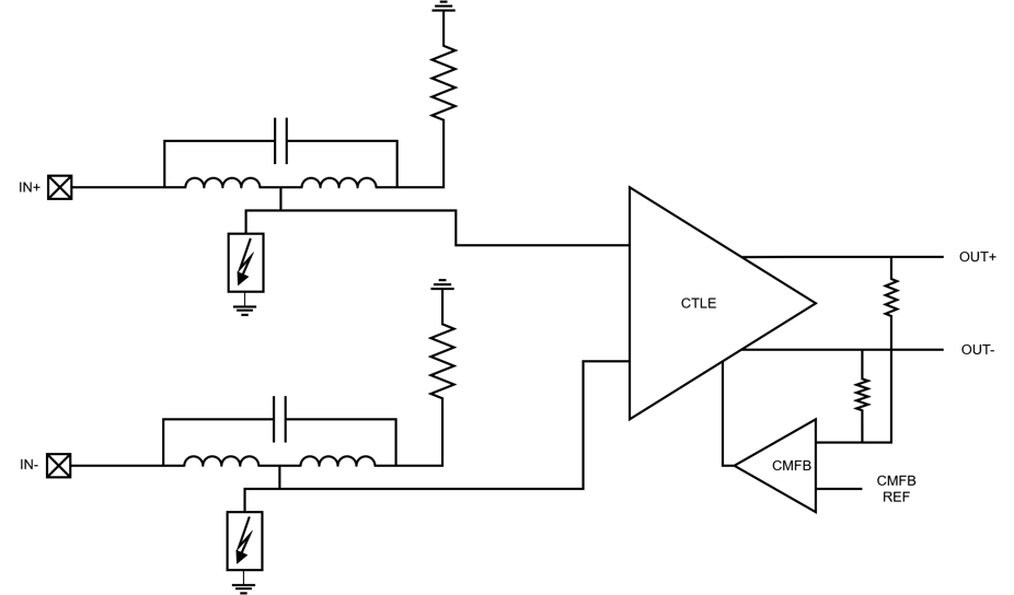
A high-speed receiver needs to handle the signal arriving at the pad. That same pad also needs ESD protection. If the protection adds too much capacitance, it can make the receiver’s job harder.
Sofics works on both sides of that problem. We develop analog front ends (AFEs), drivers, receivers and CTLEs, as well as low-capacitance ESD protection. Designing the circuit and its protection together lets us consider signal performance, area and robustness from the start.
Working on a high-speed interface?
Contact us at bd@sofics.com to discuss your signal path, package and ESD requirements.
AFE and ESD protection, designed together
In a conventional design flow, the receiver or driver may be finished before the ESD protection is added. That limits what the ESD designer can change. Co-design gives us room to look at the pad, the internal circuit and the protection path together. It is particularly useful when the interface is sensitive to added capacitance or when internal nodes need protection.
For a receiver the right solution depends on the incoming signal and the channel. Sofics’ high-speed IP portfolio includes analog front ends, CTLEs, drivers, receivers and ESD protection. The choice of circuits and protection is made for the interface requirements a CTLE is not necessarily part of every AFE.
Three ways to protect a high-speed interface
The pad needs ESD protection, but it is also the start of the signal path. These drawings show three circuit approaches: a standard arrangement, a Sofics low-capacitance ESD option and an analog front end (AFE) designed together with its protection.
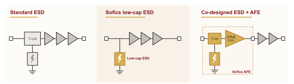
In the standard arrangement, the signal passes through a T-coil before the receiver chain, with a separate ESD path connected at the input. A low capacitance ESD clamp can be place to increase the bandwidth.
With Sofics low-cap ESD, removing the T-coil may be an option, depending on the interface. Sofics can also provide the ESD protection while the customer designs the T-coil or other parts of the AFE.
In the co-designed AFE, Sofics designs the T-coil, ESD protection and signal conditioning together. This combines low-capacitance ESD protection with functions such as channel equalization from a CTLE and adjustable gain from a VGA.
Power, performance, area and robustness
Signal path: The AFE can be tailored to the required bandwidth, signaling standard, load and voltage domain.
ESD protection: Protection is considered alongside the functional circuit, including its effect on the signal path and any sensitive internal nodes.
Area: The circuit and protection must fit the available space. Co-design enables optimized footprint.
Example: a FinFET die-to-die interface
In one die-to-die project, the request called for 2Gbps per pad across more than 5,000 instances. That adds up to more than 10Tbps across the interface. With so many instances, the space available for each one mattered.
| Footprint type | Area |
|---|---|
| Requested footprint per instance | 45 × 15µm |
| ESD portion of the solution | 25 × 10µm |
| Driver/receiver portion | 10 × 10µm |
| Total solution footprint | 35 × 10µm |
| ESD requirement | 50V CDM |
The total solution used half of the requested area per instance.
A published AFE example: TSMC 4nm
The TSMC 4nm, 0.75V die-to-die AFE datasheet describes a separate configuration with integrated ESD protection. One IP block supports organic laminate connections and advanced packages, including interposer, bridge and hybrid bonding implementations.
| Parameter | Value |
|---|---|
| Supply | 0.75V ±10% |
| Rise and fall time (10–90%) | <50ps each* |
| ESD robustness | 250V HBM |
| IO/AFE area | 625µm²** |
* Measured at the receiver pad using an identical D2D I/O circuit as the receiver, with 5dB channel loss at Nyquist.
** Area strongly depends on the required ESD protection level.
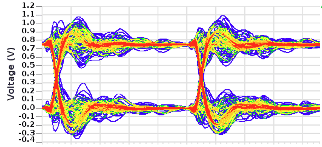
This datasheet is one example of what can be built. If your channel, packaging or protection target differs tell us what the interface needs to do.
Example: Transformer-based AFE with co-designed ESD protection
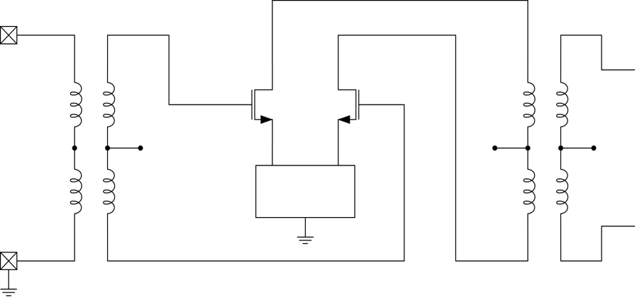
Transformer-based analog front ends present a particular challenge for ESD protection. While transformer inputs are typically highly robust against Human Body Model (HBM) events, they can be vulnerable to Charged Device Model (CDM) discharges.
The limitation of conventional ESD protection
Adding a separate ESD clamp is not always sufficient. The available placement area is restricted, CDM discharge currents can be difficult to predict, and the protection must stay within a strict capacitance budget to avoid compromising RF performance.
How Sofics approaches the problem
Instead of limiting ESD protection to a separate clamp, Sofics co-designs the protection with the transformer-based AFE.
By considering a larger portion of the circuit, rather than only the conventional clamp region, this approach enables:
- More efficient ESD protection through an optimized protection strategy.
- More predictable CDM behavior by considering discharge paths throughout the circuit.
- Reduced silicon area by integrating protection into the overall AFE design.
Optimizing beyond ESD robustness
Co-design also provides more freedom to optimize important RF-system specifications, including bandwidth, output power, power consumption and noise.
The result is an AFE design approach that considers ESD robustness and RF performance together, rather than treating protection as an additional constraint after the circuit has been developed.