Electrostatic Discharge (ESD) events occuring during the manufacturing and assembly of semiconductor devices can easily damage integrated circuits. Advanced processes like 40nm, 22nm or FinFET circuits are very vulnerable for ESD stress. Therefore, IC designers insert on-chip ESD protection devices at every chip interface of their design.

There are many different approaches used for ESD protection. It is important to select the right approach for each interface and power domain. In many design teams, on-chip ESD protection is somewhat an afterthought. They postpone ESD decisions till the start of the physical design stage. However, doing it timely can provide several benefits.
This article provides a short introduction about different concepts used in the industry.
Conventional approach
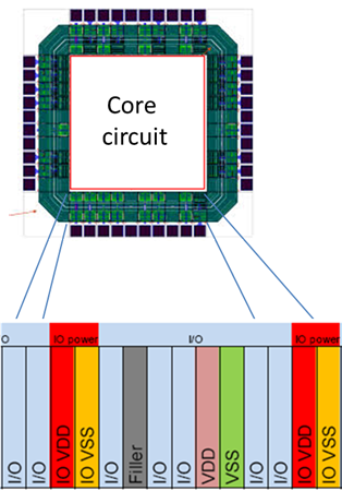
Every foundry provides a library of digital and analog I/Os. On-chip ESD protection cells are integrated within these I/O cells and also in the power/ground pads.
Most foundries apply the conventional approach that consists of these elements
- RC-triggered BigFET railclamps in the power/ground pads
- Self-protected output drivers for the digital I/Os
- Dual-diode based ESD protection for the analog I/Os
- Diodes between the grounds of different power domains

For general purpose interfaces this conventional approach is good enough. However, for high-end applications this approach is introducing limitations.
- The foundry provided GPIO library typically does not include a solution for interfaces running at the core voltage (1V-1.2V) or interface circuits based on thin oxide transistors. In the most advanced CMOS and FinFET processes, the rail clamp approach is not effective in protecting those sensitive elements. The total voltage drop across the rail clamp, bus resistance and diode is higher than the failure voltage of the core transistors. more information in another article (link)
- On the other hand, some applications require 5V tolerance, even in advanced CMOS/FinFET. the GPIO voltage range does not include that.
- The conventional approach can introduce a lot of leakage, which is bad news for battery powered applications, for IoT sensors that cycle power frequently or for high-impedance inputs. High leakage at the interface pads also deteriorates the Q-factor of LNA circuits.
- The parasitic capacitance (>200fF) of the standard analog I/O prevents IC designers to create circuits with real high bandwidth.
- General purpose I/O libraries of course also include ESD protection. Most of the time they are designed for 2kV HBM. However, some applications really need higher ESD robustness.
- For die-2-die interfaces with Through-silicon-via (TSV), the I/Os can be scattered around the die. Creating a ‘small’ local I/O segment based on the conventional approach (dual-diode + railclamp) wastes a lot of area.
Dual diode protection
The dual diode based ESD protection is probably the best known ESD protection concept for analog I/Os. It is simple, easy to transfer to any fab/process, occupies a small area and has low leakage and low parasitic capacitance.

However, the dual diode approach requires an effective and efficient rail clamp for 2 of the 4 stress cases. This means that the distance (and resistance of the Vdd/Vss bus) from the I/O to the power pads must be limited.
- ESD stress from Input to Vdd uses the upper diode.
- ESD stress from Vss to Input uses the lower diode
- ESD stress from Input to Vss however, uses the upper diode and the rail clamp
- ESD stress from Vdd to Input also uses the rail clamp and the lower diode
Of course there are additional stress cases that involve other I/Os or other power domains. Those stress combinations also frequently rely on the power/rail clamps.
There are several issues (link) with this approach.
- Circuits based on thin oxide transistors in FinFET technology cannot be protected using the diode + rail clamp approach. The total voltage drop across all these ESD elements is larger than the failure voltage of the functional circuit.
- Some applications like HDMI, DisplayPort, USB require much higher ESD robustness for the interface pads (8kV HBM) while keeping the rest of the GPIO pads at the standard 2kV requirement. In the dual diode approach this means that also the railclamp must be scaled up to allow the higher peak current.
- The diode up from Input to Vdd prevents the creation of fail-safe, hot-swap, cold-spare, over-voltage tolerance interfaces.
Sometimes it is better to protect interface circuits within the I/O area, for instance when the circuit is based on thin oxide devices and thus can fail at a low voltage.
Secondary protection
When the interface circuit is very sensitive (link) during ESD stress (low failure voltage) designers cannot use a dual diode protection approach. Fortunately, when the circuit operation can tolerate an isolation resistance between the bond pad and the circuit, then a simple approach called “secondary protection” can drasticallly extend the ESD design window.

ESD stress applied at IN versus Vss will first turn-on the local, secondary protection (green current path). Of course, the trigger voltage of this secondary protection clamp needs to be lower than the failure voltage of the circuit. ESD current through this clamp will build-up voltage across the isolation resistance, while protecting the circuit. The higher voltage at the IN pad will then trigger the primary protection (red current path).
The secondary protection clamp can be a small clamp. The size depends on the isolation resistance. If the circuit can tolerate 200 Ohm the secondary clamp can be really small. 5mA of ESD current through the secondary clamp generates 1V extra design window. This technique can enable dual diode protection for thin oxide based circuits. Frequently this secondary clamp is also called ‘CDM’ clamp because it can provide extra protection during CDM stress.

Sometimes IC designers use a second set of diodes behind the isolation resistance (figure below). At Sofics we do not like this two-stage protection. The gain from the secondary is rather limited in this case.

Self-protected output drivers
For decades IC designers have relied on ESD protection integrated into output drivers. Parasitic bipolar NPN and PNP transistors inside NMOS and PMOS devices turn on during ESD events and can protect the circuit. In mature technology nodes, those NPN/PNP devices scored well on the “ESD robustness per area” metric. Even the dual diode concept is integrated in the transistors. Down to about 90nm CMOS processes these self-protective (core) output drivers could also protect thin oxide core input gates. From 65nm the Vt1 trigger voltage of the parasitic bipolar is larger than the thin oxide breakdown voltage.

There are a number of potential issues with this approach
- Additional ‘dummy’ device fingers are needed for typical 2kV HBM – total device width of several hundred um.
- To ensure uniform triggering, silicide is blocked on the drain side and the drain area is increased.
- The silicon footprint can be rather large (link)
- The leakage and parasitic capacitance is also high.
In more advanced nodes IC designers need alternatives as described in another blog article (link).
Full-local ESD protection of I/Os
When the dual diode concept is not effective, secondary protection not allowed and self-protective drivers not possible, then our engineers turn to full-local protection concepts. In that concept all the (4) stress cases are handled locally inside the I/O area.

Sofics engineers use this approach a lot. For example when our customers need ESD protection for very sensitive circuits based on thin-oxide transistors in advanced CMOS and FinFET processes. Several cases studies can be found here (link, link). The local clamp approach provides most flexibility to fine-tune the protection for each stress case. Frequently the local clamps are based on silicon controlled rectifiers (SCR) to ensure that the silicon area remains small.
Semi-local ESD protection of I/Os
Sometimes the ESD design window is not really symmetric. The failure voltage for stress between Vdd and I/O pad can be different from the failure voltage for stress between I/O pad and Vss.
- There is a difference between NMOS and PMOS transistors during ESD stress. NMOS devices have deeper snapback than PMOS and are thus more prone to non-uniform triggering. The failure voltage for stress from output to Vss (NMOS device) is then lower than for stress between Vdd and output (PMOS device).
- When people use an open-drain interface, like for I²C there is no circuit (on the chip) between pad and Vdd. A protection clamp and diode between pad and Vss and is enough.
- For die-2-die interfaces it is not always possible to route the Vdd bus into the I/O area of the chip.
In those cases, IC designers can use the semi-local ESD protection scheme.

Conclusion
Clearly there are many different ESD protection concepts that IC designers can use for ESD protection in CMOS processes. Selecting the right approach can reduce required area, enable high performance (bandwidth) circuits and increase ESD robustness.
Contact us if you like to discuss the best approach for your own IC design.
Next articles…
Follow Sofics on LinkedIn, Facebook or Twitter to stay up-to-date about our next articles, tutorials and videos.