Semiconductor companies are developing ever faster interfaces to satisfy the need for higher data throughputs. However, the parasitic capacitance of the traditional ESD solutions limits the signal frequency. This paper demonstrates low-cap Analog I/Os for high speed SerDes (28Gbps to 112Gbps) circuits created in advanced BiCMOS, SOI and FinFET nodes.
This presentation was delivered to the 1st International EOS/ESD Symposium on Design and System (IEDS) in June 2021. IEDS is dedicated to the fundamental understanding of issues related to electrostatic discharge on design and system and the application of this knowledge to the solution of problems.
The full paper can be viewed or downloaded here
The slides can be browsed below.
Introduction
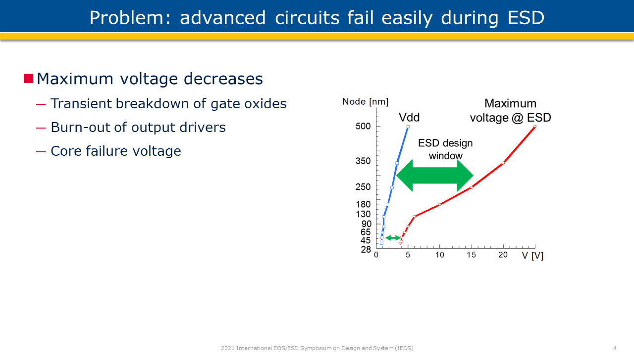
A few years ago, the speed limit was in the order of 10 Gbps. Recent circuits run at 56Gbps or even 112Gbps. For such high-speed communication interfaces chip designers need to limit the parasitic capacitance of the on-chip ESD protection clamps connected to the interfaces. Because the traditional ESD approach is not good enough, they need special analog I/O circuits. This article demonstrates silicon proven ESD solutions on advanced SiGe BiCMOS, 22nm FD-SOI and 16nm and 7nm FinFET technology. Parasitic capacitance of the ESD solutions is reduced below 100fF and for some silicon photonics applications even below 20fF.
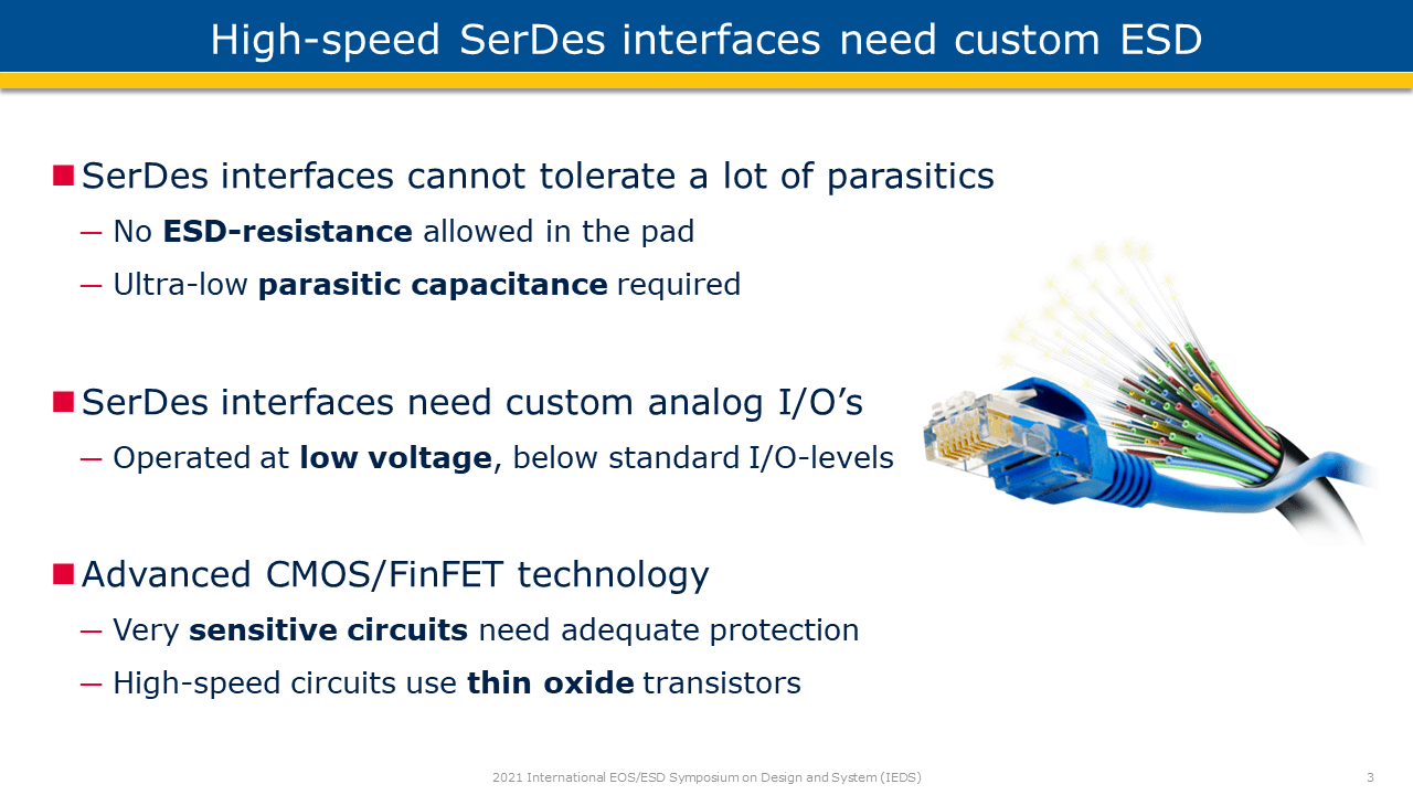
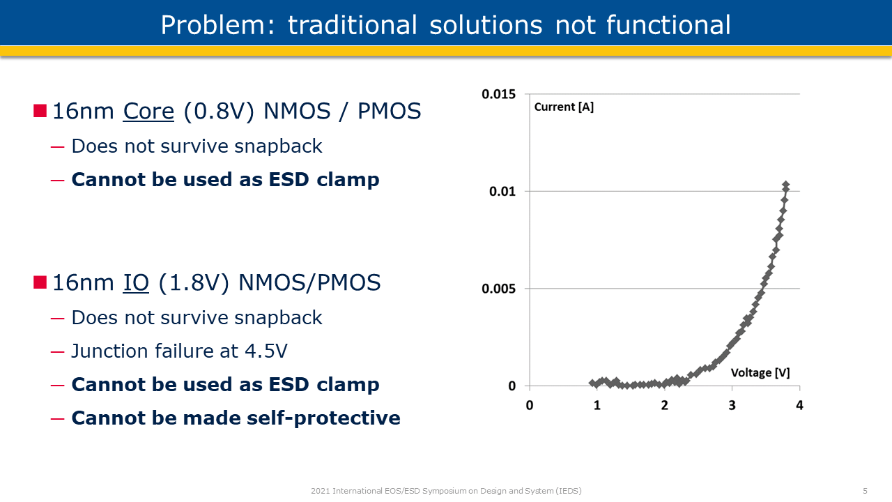
SerDes interfaces cannot tolerate a lot of parasitics. ESD protection cannot introduce resistance in the signal path and the parasitic capacitance to Vdd, Vss or substrate needs to be kept as low as possible. To design high-speed circuits, designers use the fastest transistors in the process. However these thin oxide transistors are very sensitive to ESD stress. Designers also typically use a voltage level (e.g. 1.0V or lower) below the conventional GPIO levels (1.8V, 2.5V or 3.3V).
Traditional / conventional ESD approach
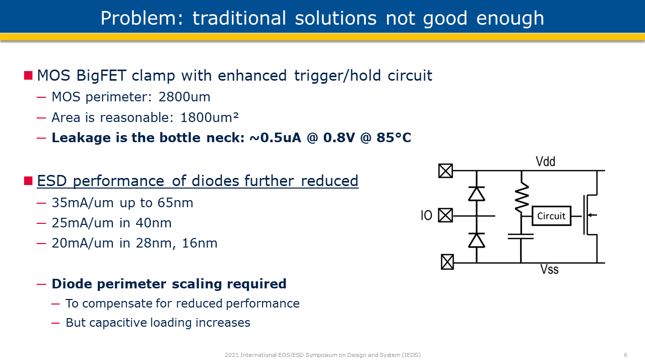
The conventional approach for ESD protection of I/Os consists of 2 diodes. A diode from Vss to the I/O pad and a diode from the I/O to Vdd. However, this approach has some issues. Designers need to ensure the rail clamp is nearby (low bus resistance). Even experts in rail clamp concepts have to admit it is very difficult to protect I/O circuits built with thin oxide transistors. Sometimes it is possible to extend the ESD design window through the secondary protection technique. However, most SerDes designers will not like to add resistance in the signal path.


Local ESD protection approach
The paper introduced the use of local ESD clamps to replace the dual ESD diode concept. This local clamp concept has some benefits like reduced dependence on the rail clamp and bus resistance. It can reduce the voltage during ESD stress. The ESD robustness can be defined for each I/O separately. The paper described several Silicon Controlled Rectifier designs with low parasitic capacitance.


Conclusions
The traditional ‘dual diode’ ESD protection concept for analog I/O pads runs into problems for the protection of high speed SerDes interfaces in advanced CMOS and FinFET nodes. The total voltage drop over diode, bus resistance and power clamp easily exceeds the failure voltage of core transistors. Moreover, the ‘diode up’ adds limitations.
This work showed several case studies where the dual diode concept was replaced with local ESD protection clamps in the I/O pad based on proprietary Diode triggered and ESD-on-SCR devices. The local clamp reduces the dependence of the bus resistance, reduces the clamping voltage and allows to optimize every analog I/O separately. Moreover, the cases show that it is possible to create ESD protection with a very low parasitic capacitance and small silicon footprint.
The data is based on dedicated ESD test chips on advanced CMOS, SOI and FinFET nodes. The analog I/Os in this work are used by more than 20 companies for the protection of high-speed SerDes interfaces in 28nm CMOS, 16nm/12nm, 7nm and 5nm FinFET technology.


Contact us if you like to discuss your own IC project.